首页
📁归档
⏳时光机
📫留言
🚩友链
💰资助名单
推荐
🎧音乐
🏜️ 壁纸
❤ 捐助
Search
1
【NPN/PNP三极管】放大电路饱和失真和截止失真的区别
19,898 阅读
2
论文写作中如何把word里面所有数字和字母替换为新罗马字体
10,511 阅读
3
【高数】形心计算公式讲解大全
8,970 阅读
4
【概论】一阶矩、二阶矩原点矩,中心矩区别与概念
7,721 阅读
5
Vivado-FPGA Verilog烧写固化教程
7,551 阅读
🪶微语&随笔
励志美文
我的随笔
写作办公
📡电子&通信
嵌入式&系统
通信&信息处理
编程&脚本笔记
⌨️IC&系统
FPGA&ASIC
VLSI&IC验证
EDA&虚拟机
💻电子&计算机
IP&SOC设计
机器学习
软硬件算法
登录
⌨️IC&系统(共78篇)
找到
78
篇与
⌨️IC&系统
相关的结果
- 第 6 页
2022-07-14
[Verilog]ASIC/FPGA实现边沿检测电路(上升/下降沿)
目录 1、什么是边沿检测 2、采用1级触发器的边沿检测电路设计(以下降沿为例)2.1、设计方法 2.2、Verilog实现 2.3、RTL电路 2.4、Testbench 2.5、仿真结果 3、采用2级触发器的边沿检测电路(以下降沿为例)3.1、设计方法 3.2、Verilog实现 3.3、RTL电路 3.4、Testbench 3.5、仿真结果 4、参考文献 1、什么是边沿检测 边沿检测用于检测信号的上升沿或下降沿,通常用于使能信号的捕捉等场景。 2、采用1级触发器的边沿检测电路设计(以下降沿为例) 2.1、设计方法 设计波形图如下所示: 图片 各信号说明如下: sys_clk:基准时钟信号(这里设定为50MHz,周期20ns) sys_rst_n:低电平有效的复位信号 in:输入信号,需要对其进行下降沿检测 ~in:输入信号的反相信号 in_d1:对输入信号寄存一拍 in_neg:得到的下降沿指示信号,该信号为 ind1 && ~in 对上图进行分析: 信号in是我们需要对其进行下降沿检测的信号 信号~in是将信号in反向 信号in_d1是使用寄存器寄存in信号,即对其进行打拍,或者说是同步到系统时钟域下 输入信号开始为高电平,在L2处变为低电平,产生第1个下降沿,在L5出产生第2个下降沿 A处为产生的第1个下降沿指示信号,B处为产生的第2个下降沿指示信号 由此我们可以推导出边沿检测信号产生的一般方法: 将需要检测的信号寄存一拍,同步到系统时钟域下,得到信号 in_d1 将需要检测的信号反向,得到信号 ~in 将信号 in_d1 反向,得到信号 ~in_d1 通过组合逻辑电路可以得到下降沿信号 in_neg:assign in_neg = ~in && in_d1 同样通过组合逻辑电路可以得到上升沿信号 in_pos:assign in_pos = in && ~in_d1 双边沿检测就是将上两条加(或运算)起来就可以了,化简后有:双边沿信号 in_both = in ^ ind1 2.2、Verilog实现 根据上文分析不难编写Verilog代码如下: //使用1级寄存器的下降沿检测电路 module detect_1 ( input sys_clk, //时钟(设定为 50MHz) input sys_rst_n, //复位信号(n 表示低电平有效) input in, //需要进行下降沿检测的输入信号 output in_neg //输出的下降沿指示信号 ); //reg 定义 reg in_d1; //寄存一拍的信号 assign in_neg = ~in && in_d1; //组合逻辑得到下降沿 //上升沿: assign in_pos = in && ~in_d1; //双边沿: assign in_pos = in ^ in_d1; //寄存模块,将输入信号打一拍 always@(posedge sys_clk or negedge sys_rst_n)begin if(!sys_rst_n) in_d1 <= 1'b0; //复位清零 else in_d1 <= in; //寄存一拍 end endmodule2.3、RTL电路 图片 上图为生成的RTL电路:该电路由一级D触发器+与逻辑门构成。 2.4、Testbench Testbench文件需要例化刚刚设计好的模块,并设置好激励。 `timescale 1ns/1ns //时间刻度:单位1ns,精度1ns module tb_detect_1(); //仿真模块 //输入reg 定义 reg sys_clk; reg sys_rst_n; reg in; //输出wire定义 wire in_neg; //设置初始化条件和输入激励 initial begin sys_clk = 1'b0; //初始时钟为0 sys_rst_n <= 1'b0; //初始复位 in <= 1'b0; //初始化输入信号 /*****以下部分为设置的激励,以产生2个下降沿*******/ #10 //10个时间单位后 sys_rst_n <= 1'b1; //拉高复位(此时复位无效) in <= 1'b1; //拉高输入 #20 //20个时间单位后 in <= 1'b0; //拉低输入,制造第1个下降沿 #80 //80个时间单位后 in <= 1'b1; //拉高输入 #60 //60个时间单位后 in <= 1'b0; //拉低输入,制造第2个下降沿 end //always代表重复进行,#10代表每10个时间单位 //每10个时间单位反转时钟,即时钟周期为20个时间单位(20ns) always #10 sys_clk = ~sys_clk; //例化被测试模块 detect_1 detect_1_inst ( .sys_clk (sys_clk ), .sys_rst_n (sys_rst_n ), .in (in), .in_neg (in_neg) ); endmodule 2.5、仿真结果 使用ModelSim执行仿真,仿真出来的波形如所示: 图片 从波形图可以看到: 10ns后停止复位 在第1条参考线处输入信号 in 产生了第1个下降沿信号 在第3条参考线处输入信号 in 产生了第2个下降沿信号 在第1条参考线和第2条参考线之间的产生了一个周期的下降沿指示信号 in_neg 在第3条参考线和第4条参考线之间的产生了一个周期的下降沿指示信号 in_neg 3、采用2级触发器的边沿检测电路(以下降沿为例) 3.1、设计方法 设计波形图如下所示: 图片 各信号说明如下: sys_clk:基准时钟信号(这里设定为50MHz,周期20ns) sys_rst_n:低电平有效的复位信号 in:输入信号,需要对其进行下降沿检测 in_d1:对输入信号寄存1拍 in_d2:对输入信号寄存2拍 ~in_d1:in_d1信号的反相信号 in_neg:得到的下降沿指示信号,该信号为 ~ind1 && ind2 对上图进行分析: 信号in是我们需要对其进行下降沿检测的信号 信号in_d1是使用寄存器寄存in信号,即对其打1拍 信号in_d2是使用寄存器寄存in_d1信号,即对其打1拍 信号~in_d1是将信号in_d1反向 输入信号开始为高电平,在L2处变为低电平,产生第1个下降沿,在L5出产生第2个下降沿 A处为产生的第1个下降沿指示信号,B处为产生的第2个下降沿指示信号 输出的下降沿指示信号落后下降沿一个时钟周期,这是因为对输入信号进行了寄存以消除亚稳态 由此我们可以推导出边沿检测信号产生的一般方法: 将需要检测的信号分别寄存1拍、2拍,同步到系统时钟域下,得到信号 in_d1、in_d2 将in_d1信号反向,得到信号 ~in_d1 将in_d2信号反向,得到信号 ~in_d2 通过组合逻辑电路可以得到下降沿信号 in_neg:assign in_neg = ~in_d1 && in_d2 同样通过组合逻辑电路可以得到上升沿信号 in_pos:assign in_pos = in_d1 && ~in_d2 双边沿检测就是将上两条加(或运算)起来就可以了,化简后有:双边沿信号 in_both = in_d1 ^ in_d2 3.2、Verilog实现 根据上文分析不难编写Verilog代码如下: //使用1级寄存器的下降沿检测电路 module detect_2 ( input sys_clk, //时钟(设定为 50MHz) input sys_rst_n, //复位信号(n 表示低电平有效) input in, //需要进行下降沿检测的输入信号 output in_neg //输出的下降沿指示信号 ); //reg 定义 reg in_d1; //寄存1拍的信号 reg in_d2; //寄存2拍的信号 assign in_neg = ~in_d1 && in_d2;//组合逻辑得到下降沿 //上升沿: assign in_pos = in && ~in_d1; //双边沿: assign in_pos = in ^ in_d1; //寄存模块,将输入信号打1拍、打2拍 always@(posedge sys_clk or negedge sys_rst_n)begin if(!sys_rst_n)begin in_d1 <= 1'b0; //复位清零 in_d2 <= 1'b0; end else begin in_d1 <= in; //寄存1拍 in_d2 <= in_d1; //寄存2拍 end end endmodule3.3、RTL电路 图片 上图为生成的RTL电路:该电路由2级D触发器+与逻辑门构成。 3.4、Testbench Testbench文件同2.4章。 3.5、仿真结果 使用ModelSim执行仿真,仿真出来的波形如所示: 图片 从波形图可以看到: 10ns后停止复位 在第1条参考线处输入信号 in 产生了第1个下降沿信号 在第4条参考线处输入信号 in 产生了第2个下降沿信号 在第2条参考线和第3条参考线之间的产生了一个周期的下降沿指示信号 in_neg 在第5条参考线和第6条参考线之间的产生了一个周期的下降沿指示信号 in_neg 两级寄存器构成的边沿检测电路可以有效的防止亚稳态的产生,产生的使能信号会落后一个时钟周期。 4、参考文献 【从零开始走进FPGA】你想干嘛——边沿检测技术 FPGA的边沿检测 FPGA基础入门篇(四) 边沿检测电路
FPGA&ASIC
刘航宇
4年前
0
2,581
1
【Verilog】卡诺图到电路Karnaugh Map to Circuit
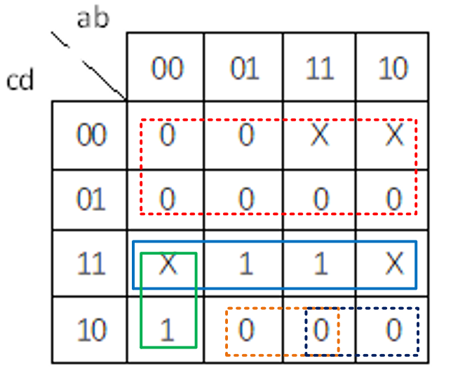
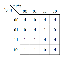
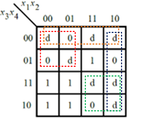
目录 问题描述一问题解答 问题描述二问题解答 问题描述三问题解答 问题描述一 具有四个输入 (a,b,c,d) 的单输出数字系统在输入出现 2、7 或 15 时产生逻辑 1,当输入出现 0、1、4、5、6、9、10、13或14 时产生逻辑 0 。数字 3、8、11 和 12 的输入条件从未出现在此系统中。例如,7 对应于分别设置a,b,c,d为0、1、1、1。确定最小SOP形式的输出out_sop,以及最小POS形式的输出out_pos。 问题解答 (1)根据题意可以画出如下卡诺图: 图片 (2)随后进行卡诺图的化简: 最小SOP:采用圈1法,如图中蓝色和绿色实线所示,合并标1的最小项,即。 最小POS:采用圈0法,如图中红、黄、深蓝色虚线所示,合并标0的最小项,得到$L=c d+\bar{a} \bar{b} c$ 通过将该逻辑表达式进行化简,可以得到。$L=c \cdot(\bar{b}+\bar{c}+d) \cdot(\bar{a}+\bar{c}+d)$ 得到该卡诺图的逻辑表达式后,便可以开始编写verilog代码。 module top_module ( input a, input b, input c, input d, output out_sop, output out_pos ); assign out_sop = (c&d)|(~a&~b&c); //sop assign out_pos = c&(~b|~c|d)&(~a|~c|d); //pos endmodule问题描述二 得出下面卡诺图中显示的函数 f。 图片 问题解答 采用圈0法,如下图所示。 图片 合并标0的最小项,得到$\bar{L}=\overline{x_{1}} \overline{x_{3}}+\overline{x_{3}} \overline{x_{4}}+x_{1} \overline{x_{2}}+x_{1} x_{3}$将该表达式化简,可以得到:$L=\left(x_{1}+x_{3}\right) \cdot\left(x_{3}+x_{4}\right) \cdot\left(\bar{X}_ {1}+x_{2}\right) \cdot\left(\bar{X}_{1}+\bar{X}_{3}\right)$得到该卡诺图的逻辑表达式后,便可以开始编写verilog代码。 module top_module ( input [4:1] x, output f ); assign f = (x[1]|x[3])&(x[3]|x[4])&(~x[1]|x[2])&(~x[1]|~x[3]); endmodule问题描述三 得出下面卡诺图中显示的函数 f。(原试题要求简化 SOP 和 POS 形式的函数。) 图片 问题解答 最小SOP:采用圈1法,如下图所示。 图片 合并标1的最小项,得到$L=\overline{x_{2}} \overline{x_{4}}+\bar{X}_ {1} x_{3}+x_{2} x_{3} x_{4}$ 最小POS:采用圈0法,如下图所示。 图片 合并标0的最小项,得到$\bar{L}=\overline{x_{3}} \overline{x_{4}}+x_{2} \overline{x_{3}}+x_{1} x_{2} \overline{x_{4}}+x_{1} \overline{x_{2}} x_{4}$,通过化简该逻辑表达式,可以得到:$L=\left(x_{3}+\overline{x_{4}}\right) \cdot\left(\overline{x_{2}}+x_{3}\right) \cdot\left(\overline{x_{1}}+\overline{x_{2}}+x_{4}\right) \cdot\left(\overline{x_{1}}+x_{2}+\overline{x_{4}}\right)$得到该卡诺图的逻辑表达式后,便可以开始编写verilog代码。 module top_module ( input [4:1] x, output f ); //assign f = (~x[2]&~x[4])|(~x[1]&x[3])|(x[2]&x[3]&x[4]); //sop assign f = (x[3]|~x[4])&(~x[2]|x[3])&(~x[1]|~x[2]|x[4])&(~x[1]|x[2]|~x[4]); //pos endmodule
FPGA&ASIC
刘航宇
4年前
0
913
1
2022-07-06
【IC设计】数字IC设计流程及学习指南
IC的设计过程可分为两个部分,前端设计(也称逻辑设计)和后端设计(也称物理设计)并没有统一严格的界限,涉及到与工艺有关的设计就是后端设计。 目录 数字IC设计流程1. 规格制定 2. 详细设计 3. HDL编码 4. 仿真验证 5. 逻辑综合――Design Compiler5.1. STA 5.2. 形式验证 技能图解 1.语言 2.基础知识 3.设计工具 4.相关岗位 数字IC设计流程 1. 规格制定 芯片规格,也就像功能列表一样,是客户向芯片设计公司(称为Fabless,无晶圆设计公司)提出的设计要求,包括芯片需要达到的具体功能和性能方面的要求。 2. 详细设计 Fabless根据客户提出的规格要求,拿出设计解决方案和具体实现架构,划分模块功能。目前架构的验证一般基于SystemC语言,对构架模型的仿真可以使用SystemC的仿真工具。其中典型的例子是Synopsys公司的CoCentric和Summit公司的Visual Elite等。 3. HDL编码 使用硬件描述语言(VHDL,Verilog HDL,业界公司一般都是使用后者)将模块功能以代码来描述实现,也就是将实际的硬件电路功能通过HDL语言描述出来,形成RTL(寄存器传输级)代码。 设计输入工具:具有强大的文本编辑功能,多种输入方法(VHDL,Verilog,状态转移图,模块图等),语法模板,语法检查,自动生产代码和文档等功能。如Active-HDL,VisualVHDL/Verilog等。 RTL分析检查工具:Synopsys LEDA 4. 仿真验证 仿真验证就是检验编码设计的正确性,检验的标准就是第一步制定的规格。看设计是否精确地满足了规格中的所有要求。规格是设计正确与否的黄金标准,一切违反,不符合规格要求的,就需要重新修改设计和编码。 设计和仿真验证是反复迭代的过程,直到验证结果显示完全符合规格标准。 仿真验证工具Synopsys的VCS,Mentor ModelSim,Cadence Verilog-XL,Cadence NC-Verilog。 5. 逻辑综合――Design Compiler 仿真验证通过,进行逻辑综合。逻辑综合的结果就是把设计实现的HDL代码翻译成门级网表netlist。综合需要设定约束条件,就是你希望综合出来的电路在面积,时序等目标参数上达到的标准。逻辑综合需要基于特定的综合库,不同的库中,门电路基本标准单元(standard cell)的面积,时序参数是不一样的。所以,选用的综合库不一样,综合出来的电路在时序,面积上是有差异的。 一般来说,综合完成后需要再次做仿真验证(这个也称为后仿真,之前的称为前仿真)逻辑综合工具Synopsys的Design Compiler(DC),Cadence的 PKS,Synplicity的Synplify等。另外,和综合工具配合使用的还有很多其他工具,如静态时间分析工具,等效性检查工具等等。Synopsys公司和Cadence公司都提供完整的工具包。 5.1. STA Static Timing Analysis(STA),静态时序分析,这也属于验证范畴,它主要是在时序上对电路进行验证,检查电路是否存在建立时间(setup time)和保持时间(hold time)的违例(violation)。这个是数字电路基础知识,一个寄存器出现这两个时序违例时,是没有办法正确采样数据和输出数据的,所以以寄存器为基础的数字芯片功能肯定会出现问题。STA工具有Synopsys的Prime Time。 5.2. 形式验证 这也是验证范畴,它是从功能上(STA是时序上)对综合后的网表进行验证。常用的就是等价性检查(Equivalence Check)方法,以功能验证后的HDL设计为参考,对比综合后的网表功能,他们是否在功能上存在等价性。这样做是为了保证在逻辑综合过程中没有改变原先HDL描述的电路功能。形式验证工具有Synopsys的Formality。前端设计的流程暂时写到这里。从设计程度上来讲,前端设计的结果就是得到了芯片的门级网表电路。 技能图解 图片 1.语言 主流的Verilog、VHDL Verilog语言与软件语言最大的区别就是,因为它是用于描述电路的,因此它的写法是非常固定的,因为电路的变化是非常有限的。学习Verilog的时候,很多时候我们并不是在学习这门语言本身,而是学习其对应的电路特征,以及如何对这个电路进行描述。如果心中没有电路,那么你是不可能写好Verilog的。 VHDL语言的严谨性比Verilog要好,不像Verilog中一样存在大量符合语法却永远无法综合的语句。 SpinalHDL、Myhdl等 SpinalHDL和Chisel师承一脉,都是基于Scala来进行电路描述。其本质上仍旧是HDL而非HLS,在设计之前依旧需要有清晰的电路结构,只不过是在电路描述上更加方便和快捷而已。 目前有一些公司已经应用于FPGA设计中,ASIC应用还有待探究。 SpinalHDL资料: https://spinalhdl.github.io/SpinalDoc-RTD/master/index.html SystemVerilog/SystemC : 这两种语言都是为了验证而存在的,掌握基本的验证方法学有助于提高自己的debug效率,SystemVerilog是一种面向对象的语言,其设计的本意是用于搭建验证平台,主流的UVM方法也都是基于SystemVerilog实现的,所以立志成为IC验证工程师的同学,SystemVerilog的深入学习和流行方法论的学习都是必不可少的。 而对于那些只想做IC设计的同学而言,SystemVerilog同样也是值得学习的。且不说本文前面提到的用于提高验证效率的debug方法,即使只是为了做好设计,SystemVerilog也是大有用武之地。很多顶级的IC设计公司内部都开始使用SystemVerilog进行RTL设计了。 由于在SystemVerilog中加入了很多类似always_ff、always_comb等用于显式表明综合电路意图的新语法,代码的可读性更高,综合过程中也减少了歧义,尽可能地保证了综合结果与设计意图的一致性。从另一个角度来说,assertion的加入也极大地提高了代码的debug效率,非常有助于在大规模的数据交互过程中定位到出错的初始点,没有掌握的同学可以多花一些时间学习一下。 -> SV基础知识 脚本语言:Makefile/Perl/Python/Shell Makefile/Perl/Python/Shell都是常用的脚本语言,进行批量修改文本内容,实现自动化操作等,掌握一门得心应手的脚本语言将对工作效率的提升帮助极大。但凡做过一次的事情,就没有必要重复第二次。 -> Perl在IC中的应用 脚本语言:Tcl 在IC设计这个领域中,Tcl是一门非常常见的语言。可以用于描述时序和管脚约束文件,UPF信息,也可以用来搭建简单的工作平台。既是很多EDA工具默认支持的脚本语言,也是这些工具配置和输出的文件格式。因此,能够读懂Tcl,掌握Tcl语言的基本语法,就可以帮助更好的使用EDA工具。 -> 从零开始学Tcl C语言 作为基础语言,在验证时,往往需要用到C写的case; 2.基础知识 数电模电、电路分析、数据结构、计算机体系架构等 AMBA总线 AXI、AHB、APB、CHI、ACE等; -> AMBA总线 高低速接口 PCIE、DMA、DDR、USB、UART、SPI、I2C、MIPI等 -> 总线接口 低功耗设计 动态功耗、静态功耗、常见低功耗设计方法 -> 低功耗设计 静态时序分析 建立时间、保持时间、亚稳态及其解决方法、时序约束 -> 时序约束策略 、亚稳态、 FPGA中的亚稳态 设计方法 乒乓操作、流水线、串并转换、无毛刺切换、状态机等 跨时钟处理:快到慢、慢到快、异步FIFO(FIFO深度计算)等 ->时钟切换电路(Glitch-free clock switching circuit)、异步FIFO、同步FIFO、同步和异步FIFO、FIFO深度计算 3.设计工具 linux系统:linux、shell常见命令 gvim/emac编辑器: 熟练使用Vim/Emacs,用编程的方式来编程,可以提高效率。 版本管理工具:SVN、Git、p4等 版本管理,简而言之,就是一种用于记录和查询文件版本改动的工具; EDA工具 仿真工具:NCVerilog/ VCS/ ModelSim/ iVerilog 以上是比较业界比较主流的仿真工具,其中Icarus Verilog (iVerilog)为开源工具,仿真过程需要了解: 如何指定编译的文件类型; 如何指定编译文件清单; 如何指定索引目录; 如何指定仿真精度; 如何指定临时的宏变量; 如何指定语法检查的严苛等级; 如何混合编译由多种语言写成的工程; 如何调用不同波形生成工具的pli接口; 如何配合SDF反标进行后仿等; -> 芯片后仿及SDF反标、VCS实用技巧、开源verilog仿真工具iverilog+GTKWave 波形查看工具:DVE/ Verdi/ gtkWave 以上是业界比较主流的波形查看工具,所有的波形查看器都必须支持标准波形文件.vcd格式,但是由于.vcd格式的存储性能并不好,冗余信息过多,所以各波形查看工具都纷纷推出了自己支持的波形文件格式,如DVE的.vpd,Verdi的.fsdb,ModelSim的*.wlf; gtkWave也是跨平台的,而且简单易用,支持.vcd标准格式,同时支持高性能压缩格式.lxt和*.fst,gtkWave自带vcd转fst的转换器; 通常几G左右的.vcd格式波形转换为.vpd格式后只有几十MB左右,而转换为.fsdb后通常会更小,因此将标准波形文件.vcd转换为其他压缩格式更加有利于数据备份。 -> fsdb实用技巧、verdi实用技巧 逻辑等效性检查工具:formality-> 形式验证与formality基本流程 从功能上对综合后的网表进行验证,常用的就是等价性检查方法,以功能验证后的HDL设计为参考,对比综合后的网表功能,他们是否在功能上存在等价性。这样做是为了保证在逻辑综合过程中没有改变原先HDL描述的电路功能。 综合工具:dc ->DC综合 逻辑综合就是将HDL代码翻译成门级网表netlist; lint/cdc检查工具:spyglass -> SpyGlass安装教程、spyglass 基础操作、spyglass 常见错误lint 后端:PT、IIC2、innovus等 FPGA综合布线布局工具:synplify/vivado-> ->synplify 基础操作、基于synplify+vivado生成bitfile 其他:VC_static_tools ->VC_static Tools安装教程 4.相关岗位 前端设计 RTL IP设计:从算法协议到RTL coding的能力; SoC设计集成/验证:总线、功耗、系统架构的能力; SOC侧重将IP,模块集成形成一个系统,所以片上互联总线和外设接口是掌握的重点。片内互联总线一般是AMBA总线。外设接口又分为低速接口和高速接口,其中低速接口包括I2C,UART,SPI等,高速接口包括SATA,USB,PCIE,DDR等; 验证 FPGA原型验证:HAPS -> HAPS®-100原型系统、芯片验证技术 |HAPS与高性能ASIC原型验证 UVM验证:SV、UVM主流验证方法学 ->UVM芯片验证 EMU验证:zebu、帕拉丁 -> 芯片验证应用|基于ZeBu平台的虚拟主机应用方案 综合: 逻辑综合就是将HDL代码翻译成门级网表netlist; STA Static Timing Analysis(STA),静态时序分析,它主要是在时序上对电路进行验证,检查电路是否存在建立时间(setup time)和保持时间(hold time)的违例(violation),一个寄存器出现这两个时序违例时,是没有办法正确采样数据和输出数据的,所以以寄存器为基础的数字芯片功能肯定会出现问题。 DFT Design ForTest,可测性设计。芯片内部往往都自带测试电路,DFT的目的就是在设计的时候就考虑将来的测试。DFT的常见方法就是,在设计中插入扫描链,将非扫描单元(如寄存器)变为扫描单元;如bist、Scan Design、JTAG、ATPG等; 后端 物理验证、布线布局、静态时序分析、等价性检查、功耗分析
FPGA&ASIC
# ASIC/FPGA
刘航宇
4年前
0
3,043
9
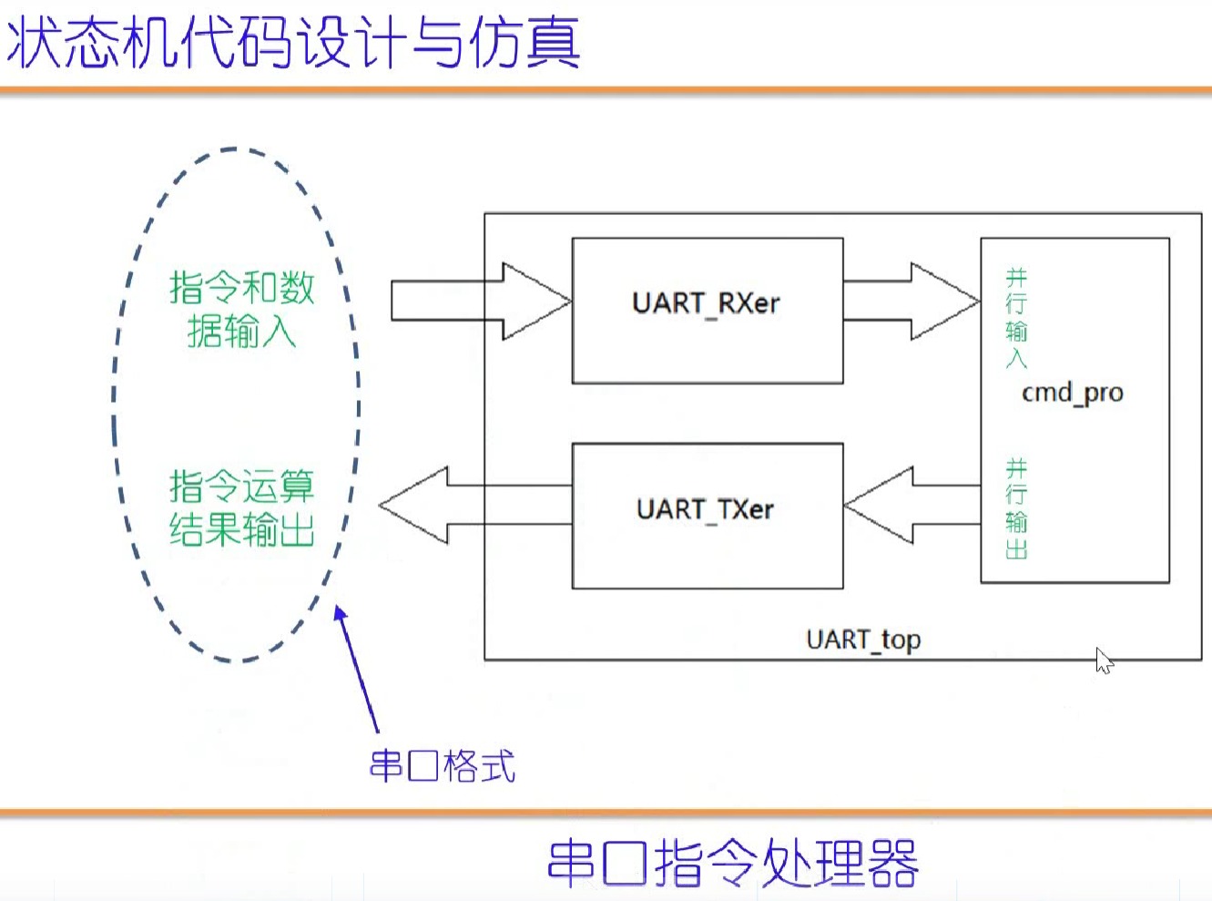
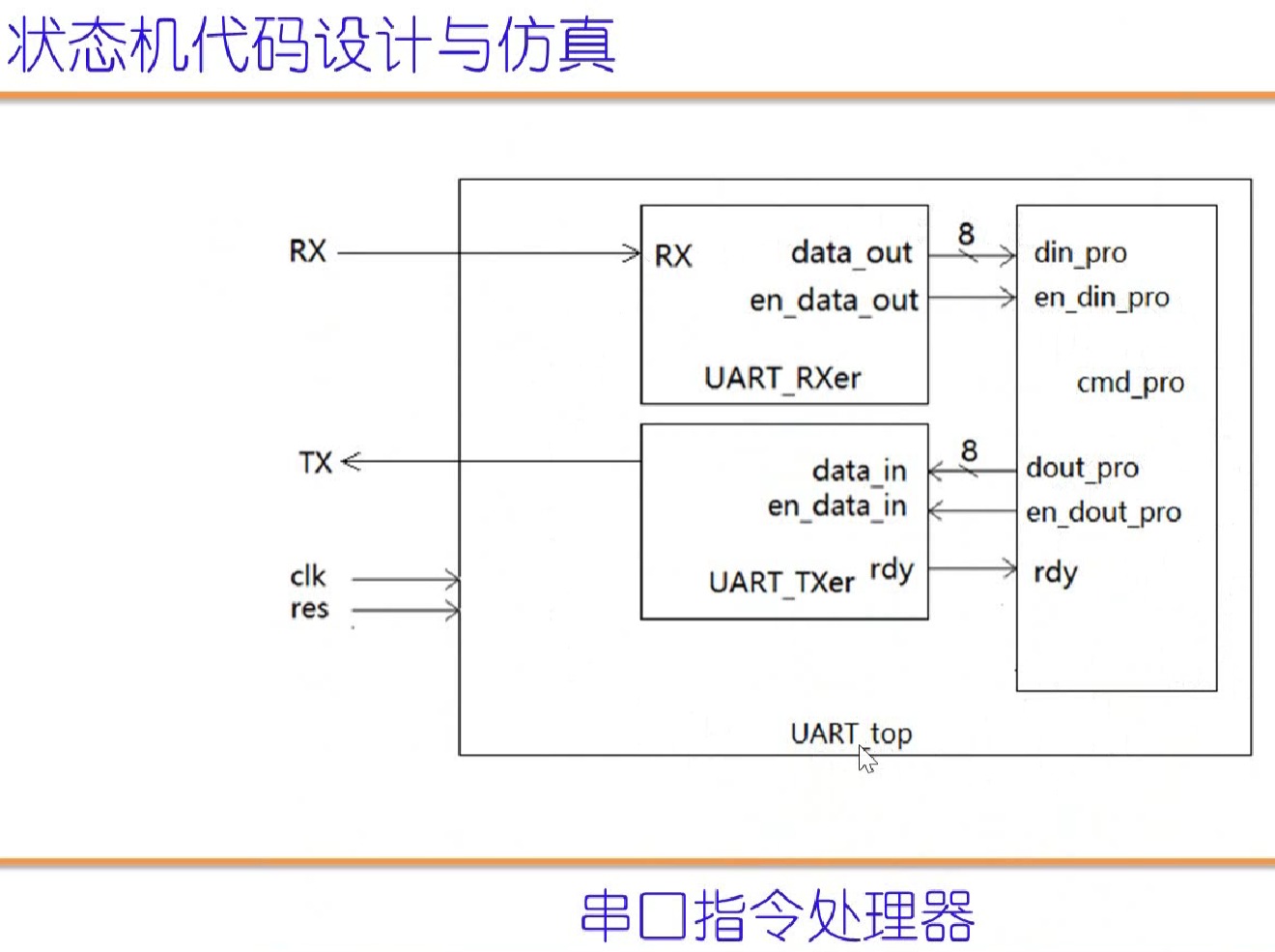
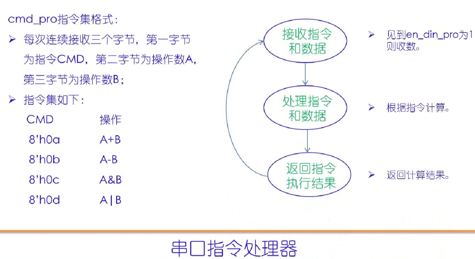
【9】Verilog练习-串口指令处理器
目录 理论: 代码cmd_pro UART_top 现象 理论: 图片 图片 图片 代码 RX、TX需要与之在相同目录下 cmd_pro //指令处理器 `timescale 1ns/10ps module cmd_pro( clk, res, din_pro, en_din_pro, dout_pro, en_dout_pro, rdy ); input clk; input res; input[7:0] din_pro;//指令和数据输入端口; input en_din_pro;//输入使能; output[7:0] dout_pro;//指令执行结果; output en_dout_pro;//指令输出使能; output rdy;//串口发送模块空闲标志,0表示空闲; parameter add_ab=8'h0a; parameter sub_ab=8'h0b; parameter and_ab=8'h0c; parameter or_ab=8'h0d; reg[2:0] state;//主状态机寄存器(2^3个状态); reg[7:0] cmd_reg,A_reg,B_reg;//存放指令、A和B; reg[7:0] dout_pro; reg en_dout_pro; always@(posedge clk or negedge res) if(~res)begin state<=0;cmd_reg<=0;A_reg<=0;B_reg<=0;dout_pro<=0; en_dout_pro<=0; end else begin case(state) 0://等指令; begin en_dout_pro<=0; if(en_din_pro) begin cmd_reg<=din_pro; state<=1; end end 1://收A; begin if(en_din_pro) begin A_reg<=din_pro; state<=2; end end 2://收B; begin if(en_din_pro) begin B_reg<=din_pro; state<=3; end end 3://指令译码和执行 begin state<=4; case(cmd_reg) add_ab: begin dout_pro<=A_reg+B_reg; end sub_ab: begin dout_pro<=A_reg-B_reg; end and_ab: begin dout_pro<=A_reg&B_reg; end or_ab: begin dout_pro<=A_reg|B_reg; end endcase end 4://发送指令执行结果 begin if(~rdy)begin en_dout_pro<=1; state<=0; end end default:// begin state<=0; en_dout_pro<=0; end endcase end endmoduleUART_top //串口指令处理器 `timescale 1ns/10ps module UART_top( clk, res, RX, TX ); input clk; input res; input RX; output TX; wire[7:0] din_pro; wire en_din_pro; wire[7:0] dout_pro; wire en_dout_pro; wire rdy; UART_Rxer UART_Rxer( .clk(clk), .res(res), .RX(RX), .data_out(din_pro), .en_data_out(en_din_pro) ); UART_TXer UART_TXer( .clk(clk), .res(res), .data_in(dout_pro), .en_data_in(en_dout_pro), .TX(TX), .rdy(rdy) ); cmd_pro cmd_pro( .clk(clk), .res(res), .din_pro(din_pro), .en_din_pro(en_din_pro), .dout_pro(dout_pro), .en_dout_pro(en_dout_pro), .rdy(rdy) ); endmodule //-----testbench of UART_top----- module UART_top_tb; reg clk,res; wire RX; wire TX; reg[45:0] RX_send;//里面装有串口字节发送数据 assign RX=RX_send[0];//连接RX; reg[12:0] con; UART_top UART_top( clk, res, RX, TX ); initial begin clk<=0;res<=0;RX_send<={1'b1,8'h09,1'b0,1'b1,8'h06,1'b0,1'b1,8'h0a,1'b0,16'hffff}; con<=0; #17 res<=1; #4000000 $stop; end always #5 clk<=~clk; always@(posedge clk)begin if(con==5000-1)begin con<=0; end else begin con<=con+1; end if(con==0)begin RX_send[44:0]<=RX_send[45:1]; RX_send[45]<=RX_send[0]; end end endmodule现象 图片
FPGA&ASIC
# ASIC/FPGA
刘航宇
4年前
0
405
2
2022-06-21
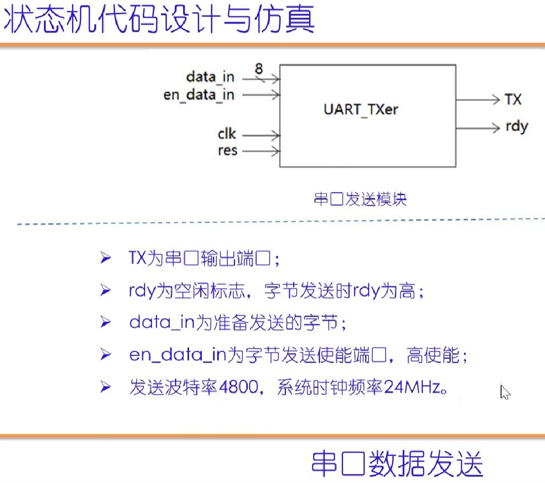
【8】Verilog练习-串口数据发送
理论: 图片 图片 代码: //串口发送模块 `timescale 1ns/10ps module UART_TXer( clk, res, data_in, en_data_in, TX, rdy ); input clk; input res; input[7:0] data_in;//准备发送的数据; input en_data_in;//发送使能; output TX;//输出使能 output rdy;//空闲标志,0表示空闲; reg[3:0] state;//主状态机寄存器; reg[9:0] send_buf;//发送寄存器 assign TX=send_buf[0];//连接TX; reg[9:0] send_flag;//用于判断右移结束; reg[12:0] con;//用于计算波特周期 reg rdy; always@(posedge clk or negedge res) if(~res)begin state<=0;send_buf<=1;con<=0;send_flag<=10'b10_0000_0000;rdy<=0; end else begin case(state) 0://等待使能信号; begin if(en_data_in)begin send_buf={1'b1,data_in,1'b0}; send_flag<=10'b10_0000_0000; rdy<=1; state<=1; end end 1://串口发送,寄存器右移; begin if(con==5000-1)begin con<=0; end else begin con<=con+1; end if(con==5000-1)begin send_buf[8:0]<=send_buf[9:1]; send_flag[8:0]<=send_flag[9:1]; end if(send_flag[0])begin rdy<=0; state<=0; end end endcase end endmodule //----testbench of UART_TXer--- module UART_TXer_tb; reg clk,res; reg[7:0] data_in; reg en_data_in; wire TX; wire rdy; UART_TXer UART_TXer( //同名例化; clk, res, data_in, en_data_in, TX, rdy ); initial begin clk<=0;res<=0;data_in<=8'h7f;en_data_in<=0; #17 res<=1; #30 en_data_in<=1; #10 en_data_in<=0; #10000 $stop; end always #5 clk<=~clk; endmodule结果: 图片
FPGA&ASIC
# ASIC/FPGA
刘航宇
4年前
0
487
3
2022-06-15
【7】Verilog练习-串口数据接收
原理: 图片 图片 图片 图片 程序 //串口数据接收 `timescale 1ns/10ps module UART_Rxer( clk, res, RX, data_out, en_data_out ); input clk; input res; input RX; output[7:0] data_out;//接收字节输出; output en_data_out;//输出使能; reg[7:0] data_out; reg[7:0] state;//主状态机; reg[12:0] con;//用于计算比特宽度; reg[3:0] con_bits;//用于计算比特数; reg RX_delay;//RX的延时; reg en_data_out; always@(posedge clk or negedge res) if(~res)begin state<=0;con<=0;con_bits<=0;RX_delay<=0; data_out<=0;en_data_out<=0; end else begin RX_delay<=RX; case(state) 0://等空闲; begin if(con==5000-1)begin //24M/4800=5000 con<=0; end else begin con<=con+1; end if(con==0)begin if(RX)begin con_bits<=con_bits+1; end else begin con_bits<=0; end if(con_bits==12)begin//连续12个1,说明处于空闲状态 state<=1; end end end 1://等起始位; begin en_data_out<=0; if(~RX&RX_delay)begin state<=2; end end 2://收最低位b0;T=5000;1.5T=7500 begin if(con==7500-1)begin con<=0; data_out[0]<=RX; state<=3; end else begin con<=con+1; end end 3://收最低位b1; begin if(con==5000-1)begin con<=0; data_out[1]<=RX; state<=4; end else begin con<=con+1; end end 4://收最低位b2; begin if(con==5000-1)begin con<=0; data_out[2]<=RX; state<=5; end else begin con<=con+1; end end 5://收最低位b3; begin if(con==5000-1)begin con<=0; data_out[3]<=RX; state<=6; end else begin con<=con+1; end end 6://收最低位b4; begin if(con==5000-1)begin con<=0; data_out[4]<=RX; state<=7; end else begin con<=con+1; end end 7://收最低位b5; begin if(con==5000-1)begin con<=0; data_out[5]<=RX; state<=8; end else begin con<=con+1; end end 8://收最低位b6; begin if(con==5000-1)begin con<=0; data_out[6]<=RX; state<=9; end else begin con<=con+1; end end 9://收最低位b7; begin if(con==5000-1)begin con<=0; data_out[7]<=RX; state<=10; end else begin con<=con+1; end end 10://产生使能脉冲 begin en_data_out<=1; state<=1; end default:// begin state<=0; con<=0; con_bits<=0; en_data_out<=0; end endcase end endmodule //----testbench of UART_Rxer-- module UART_Rxer_tb; reg clk,res; wire RX; wire[7:0] data_out; wire en_data_out; reg[25:0] RX_send;//里面装有串口字节发送数据; assign RX=RX_send[0];//连接RX reg[12:0] con; UART_Rxer UART_Rxer( .clk(clk), .res(res), .RX(RX), .data_out(data_out), .en_data_out(en_data_out) ); initial begin clk<=0;res<=0;RX_send<={1'b1,8'haa,1'b0,16'hffff}; con<=0; #17 res<=1; #4000000 $stop; end always #5 clk<=~clk; always@(posedge clk)begin if(con==5000-1)begin con<=0; end else begin con<=con+1; end if(con==0)begin RX_send[24:0]<=RX_send[25:1]; RX_send[25]<=RX_send[0]; end end endmodule现象 图片
FPGA&ASIC
刘航宇
4年前
0
494
3
【6】Verilog练习-三角波梯形波发生器
三角波发生器理论 图片 代码 //三角波发生器 `timescale 1ns/10ps module tri_gen( clk, res, d_out ); input clk; input res; output[8:0] d_out; reg state; reg[8:0] d_out; always@(posedge clk or negedge res) if(~res) begin state<=0;d_out<=0; end else begin case(state) 0://上升 begin d_out<=d_out+1; if(d_out==299)begin state<=1; end end 1://下降 begin d_out<=d_out-1; if(d_out==1)begin state<=0; end end endcase end endmodule //------testbench of tri_gen---- module tri_gen_tb; reg clk,res; wire[8:0] d_out; tri_gen U1( .clk(clk), .res(res), .d_out(d_out) ); initial begin clk<=0;res<=0; #17 res<=1; #8000 $stop; end always #5 clk<=~clk; endmodule现象 图片 梯形波发生器 //三角波发生器->改进为梯形波 `timescale 1ns/10ps module tri_gen( clk, res, d_out ); input clk; input res; output[8:0] d_out; reg[1:0] state;//3个状态2位,不在是原来的1bit reg[8:0] d_out; reg[7:0] con;//计数器,记录平顶周期个数 always@(posedge clk or negedge res) if(~res) begin state<=0;d_out<=0;con<=0; end else begin case(state) 0://上升 begin d_out<=d_out+1; if(d_out==299)begin state<=1; end end 1://平顶 begin if(con==200) begin state<=2; con<=0; end else begin con<=con+1; end end 2://下降 begin d_out<=d_out-1; if(d_out==1)begin state<=0; end end default://3状态 begin state<=0; con<=0; end endcase end endmodule //------testbench of tri_gen---- module tri_gen_tb; reg clk,res; wire[8:0] d_out; tri_gen U1( .clk(clk), .res(res), .d_out(d_out) ); initial begin clk<=0;res<=0; #17 res<=1; #20000 $stop; end always #5 clk<=~clk; endmodule现象 图片
FPGA&ASIC
刘航宇
4年前
0
804
3
2022-05-25
【5】Verilog练习-相邻16点相加
图片 图片 代码 //相邻16点相加 `timescale 1ns/10ps module sigma_16p( clk, res, data_in, syn_in, data_out, syn_out ); input clk,res; input[7:0] data_in;//采样信号 input syn_in;//采样时钟 output[11:0] data_out;//累加结果输出 output syn_out;//累加结果同步脉冲 reg syn_in_n1;//syn_in的反向延时 wire syn_pulse;//采样时钟上升沿识别脉冲 assign syn_pulse=syn_in&syn_in_n1; reg[3:0] con_syn;//采样时钟循环计数器 wire[7:0] comp_8;//补码 wire[11:0] d_12;//升位结果 assign comp_8=data_in[7]?{data_in[7],~data_in[6:0]+1}:data_in;//补码运算 assign d_12={comp_8[7],comp_8[7],comp_8[7],comp_8[7],comp_8}; reg[11:0] sigma;//累加计算 reg[11:0] data_out; reg syn_out; always@(posedge clk or negedge res) if(~res)begin syn_in_n1<=0;con_syn<=0;sigma<=0;data_out<=0;syn_out<=0; end else begin syn_in_n1<=~syn_in; if(syn_pulse)begin con_syn<=con_syn+1; end if(syn_pulse)begin if(con_syn==15)begin sigma<=d_12; data_out<=sigma; syn_out<=1; end else begin sigma<=sigma+d_12; end end else begin syn_out<=0; end end endmodule //-----testbench of sigma_16p--- module sigma_16p_tb; reg clk,res; reg[7:0] data_in; reg syn_in; wire[11:0] data_out; wire syn_out; sigma_16p sigma_16p( .clk(clk), .res(res), .data_in(data_in), .syn_in(syn_in), .data_out(data_out), .syn_out(syn_out) ); initial begin clk<=0;res<=0;data_in=1;syn_in<=0; #17 res<=1; #50000 $stop; end always #5 clk<=~clk; always #100 syn_in<=~syn_in; endmodule现象 图片
FPGA&ASIC
刘航宇
4年前
0
451
1
【4】Verilog练习-秒计数器设计
秒计数器设计 图片 代码 //秒计数器,0-9循环 `timescale 1ns/10ps module s_counter( clk, res, s_num ); input clk; input res; output[3:0] s_num; parameter frequency_clk=24;//24MHZ; reg[24:0] con_t;//秒脉冲分频计数器; reg s_pulse;//秒脉冲尖; reg[3:0] s_num; always@(posedge clk or negedge res) if(~res)begin con_t<=0;s_pulse<=0;s_num<=0; end else begin //if(con_t==frequency_clk*1000000-1)begin if(con_t==frequency_clk*1000-1)begin//仿真便于观察 con_t<=0; end else begin con_t<=con_t+1; end if(con_t==0)begin s_pulse<=1; end else begin s_pulse<=0; end if(s_pulse) begin if(s_num==9)begin s_num<=0; end else begin s_num<=s_num+1; end end end endmodule //-----testbench of s_counter--- module s_counter_tb; reg clk,res; wire[3:0] s_num; s_counter s_counter( .clk(clk), .res(res), .s_num(s_num) ); initial begin clk<=0;res<=0; #17 res<=1; #1000000 $stop; end always #5 clk<=~clk; endmodule现象 图片 扩展:数码管 图片 图片
FPGA&ASIC
刘航宇
4年前
0
456
2
2022-05-23
【3】Verilog练习-时序逻辑与伪随机码发生器设计和仿真
时序逻辑代码与仿真 图片 代码 //计数器 `timescale 1ns/10ps module counter( clk, res, y ); input clk; input res; output[7:0] y; reg[7:0] y; wire[7:0] sum;//+1运算的结果; assign sum=y+1;//组合逻辑部分; always@(posedge clk or negedge res) if(~res)begin y<=0; end else begin y<=sum; end endmodule //----testbench of counter---- module counter_tb; reg clk,res; wire[7:0] y; counter counter( .clk(clk), .res(res), .y(y) ); initial begin clk<=0;res<=0; #17 res<=1; #6000 $stop; end always #5 clk<=~clk; endmodule现象 图片 模拟显示 图片 伪随机码发生器 图片 代码 //四级伪随机码发生器; `timescale 1ns/10ps module m_gen( clk, res, y ); input clk; input res; output y; reg[3:0] d; assign y=d[0]; always@(posedge clk or negedge res) if(~res)begin d<=4'b1111; end else begin d[2:0]<=d[3:1];//右移一位; d[3]<=d[3]+d[0];//模二加; end endmodule //----testbench of m_gen---- module m_gen_tb; reg clk,res; wire y; m_gen m_gen( .clk(clk), .res(res), .y(y) ); initial begin clk<=0;res<=0; #17 res<=1; #600 $stop; end always #5 clk<=~clk; endmodule现象 图片
FPGA&ASIC
刘航宇
4年前
0
517
1
2022-05-21
【2】Verilog练习-补码转化与7段译码逻辑设计
补码转化 图片 程序 //补码转化逻辑 `timescale 1ns/10ps module comp_conv( a, a_comp ); input[7:0] a; output[7:0] a_comp; //wire[6:0] b;//按位取反的幅度位 //wire[7:0] y;//负数的补码; //assign b=~a[6:0]; //assign y[6:0]=b+1;//按位取反+1 //assign y[6:0]=~a[6:0]+1;//按位取反+1 //assign y[7]=a[7];//符号位不变 //assign y={a[7],~a[6:0]+1}; //assign a_comp=a[7]?y:a;//二选一 assign a_comp=a[7]?{a[7],~a[6:0]+1}:a;//二选一 endmodule //----testbench of comp_conv--- module comp_conv_tb; reg[7:0] a_in; wire[7:0] y_out; comp_conv comp_conv( .a(a_in), .a_comp(y_out) ); initial begin a_in<=0; #3000 $stop; end always #10 a_in<=a_in+1; endmodule现象 图片 7段译码逻辑设计 图片 代码: //七段码译码器 `timescale 1ns/10ps module seg_dec( num, a_g ); input[3:0] num; output[6:0] a_g;//a_g-->{a,b,c,d,e,f,g} reg[6:0] a_g; always@(num)begin case(num) 4'd0: begin a_g<=7'b111_1110; end 4'd1: begin a_g<=7'b011_0000; end 4'd2: begin a_g<=7'b110_1101; end 4'd3: begin a_g<=7'b111_1100; end 4'd4: begin a_g<=7'b011_0011; end 4'd5: begin a_g<=7'b101_1011; end 4'd6: begin a_g<=7'b101_1111; end 4'd7: begin a_g<=7'b111_0000; end 4'd8: begin a_g<=7'b111_1111; end 4'd9: begin a_g<=7'b111_1011; end default: begin a_g<=7'b000_0001; end//中杠 endcase end endmodule //----testbench of seg_dec--- module seg_dec_tb; reg[3:0] num_in; wire[6:0] a_g_out; seg_dec seg_dec( .num(num_in), .a_g(a_g_out) ); initial begin num_in<=0; #200 $stop; end always #10 num_in<=num_in+1; endmodule现象 图片
FPGA&ASIC
刘航宇
4年前
0
680
3
2022-05-17
【2】Verilog练习-组合逻辑电路多路选择器
目录 二选一逻辑设计 多路选择逻辑设计 二选一逻辑设计 图片 图片 程序 //二选一逻辑设计 `timescale 1ns/10ps module fn_sw( a, b, sel, y ); input a; input b; input sel; output y; //assign y=sel?(a^b):(a&b); //用always语句块实现组合逻辑; reg y; always@(a or b or sel) if(sel==1)begin y<=a^b; end else begin y<=a&b; end endmodule //---testbench of fn_sw---- module fn_sw_tb; reg a,b,sel;//输入reg型 wire y;//输出wire型 fn_sw fn_sw( .a(a), .b(b), .sel(sel), .y(y) ); initial begin a<=0;b<=0;sel<=0; #10 a<=0;b<=0;sel<=1; #10 a<=0;b<=1;sel<=0; #10 a<=1;b<=0;sel<=0; #10 a<=1;b<=0;sel<=1; #10 a<=1;b<=1;sel<=0; #10 a<=1;b<=1;sel<=1; #10 $stop; end endmodule现象 图片 多路选择逻辑设计 图片 代码 //四选一逻辑设计 `timescale 1ns/10ps module fn_sw_4( a, b, sel, y ); input a; input b; input[1:0] sel; output y; reg y; always@(a or b or sel)begin case(sel) 2'b00:begin y<=a&b;end 2'b01:begin y<=a|b;end 2'b10:begin y<=a^b;end 2'b11:begin y<=~(a^b);end endcase end endmodule //-----testbench of fn_sw_4-- module fn_sw_4_tb; reg[3:0] absel; wire y; fn_sw_4 fn_sw_4( .a(absel[0]), .b(absel[1]), .sel(absel[3:2]), .y(y) ); initial begin absel<=0; #300 $stop; end always #10 absel<=absel+1; endmodule现象 图片
FPGA&ASIC
刘航宇
4年前
0
742
2
上一页
1
...
5
6
7
下一页

![[Verilog]ASIC/FPGA实现边沿检测电路(上升/下降沿)](https://img-blog.csdnimg.cn/20210802191442636.PNG)